Innovative research progress in photonic tensor processing chip by Prof. Weiwen Zou's group at Shanghai Jiao Tong University
The group of Professor Weiwen Zou from the Department of Electronic Engineering of Shanghai Jiaotong University has developed a novel photonic tensor processing chip that realizes high-speed tensor convolution operations. The related results were published in Nature Communications in December 2022 under the title "High-order tensor flow processing using integrated photonic circuits". The research is solely completed by Shanghai Jiao Tong University, with Shaofu Xu, assistant professor, and Jing Wang, Ph.D. student, as co-first authors, and Prof. Weiwen Zou, at the Intelligent Microwave Lightwave Integration Innovation Center (imLic), Department of Electronic Engineering, as the corresponding author.

From left to right:Shaofu Xu, Jing Wang, Sicheng Yi, and Weiwen Zou
Backgrounds
The tensor form stacked from multidimensional data is an efficient form of data processing, which is conducive to discovering the intrinsic structural features in data and is widely used in radar, communication, artificial intelligence, life science and other fields. With the development of information technology and the explosive growth of data generation rate, the multidimensional stacking of massive data and its efficient and fast processing become an important scientific challenge nowadays. To meet this challenge, traditional electrical processors usually adopt the Generalized Matrix Multiplication (GeMM) strategy to transform high-order tensor operations into matrix multiplication operations. Multi-level looped operations are transformed into parallel operations, so that increasing the number of processing cores is effective to increase the throughput of tensor processing. However, the GeMM strategy relies on a large number of data replications, which requires additional memory usage and repeated communication overhead between memory and processor. It is one of the core bottlenecks to improve the speed of tensor operations on multidimensional data.
Innovation results
This study proposes an innovative interdisciplinary research idea, using integrated photonic circuits to build a tensor processor. It can take advantage of the high-speed characteristics of photonics to increase the clock frequency of processing to tens of GHz and also can use the multiple degrees of freedom of optics to directly represent multiple dimensions of tensor data. This idea eliminates the need for tensor-to-matrix transformation and enables tensor processing from input to output in a flow fashion (as shown in Figure 1). Based on this idea, the group designed and developed a photonic tensor processing chip (shown in Figure 2), which integrates the three degrees of freedom of optical wavelength, space and time delay. It successfully verified the high-speed tensor convolution operation with a clock frequency of 20 GHz on multi-channel images (shown in Figure 3), with an on-chip computing density of 588 GOPS/mm2. Increasing the scale of photonic integration will upgrade computing density over 1TOPS/mm2. The research group used the chip to build a convolutional neural network for video action recognition. The convolutional layers in the network were completed on the photonic tensor processing chip. A recognition accuracy of 97.9% was finally achieved on the KTH video data set, close to the ideal recognition accuracy of 98.9%. In summary, this research shows that the photonic integrated chip can realize tensor flow processing at ultra-high clock frequency. It solves the problem of extra memory occupation and memory accesses. It provides a new technical way to build advanced information systems such as high-performance computing and broadband signal processing.
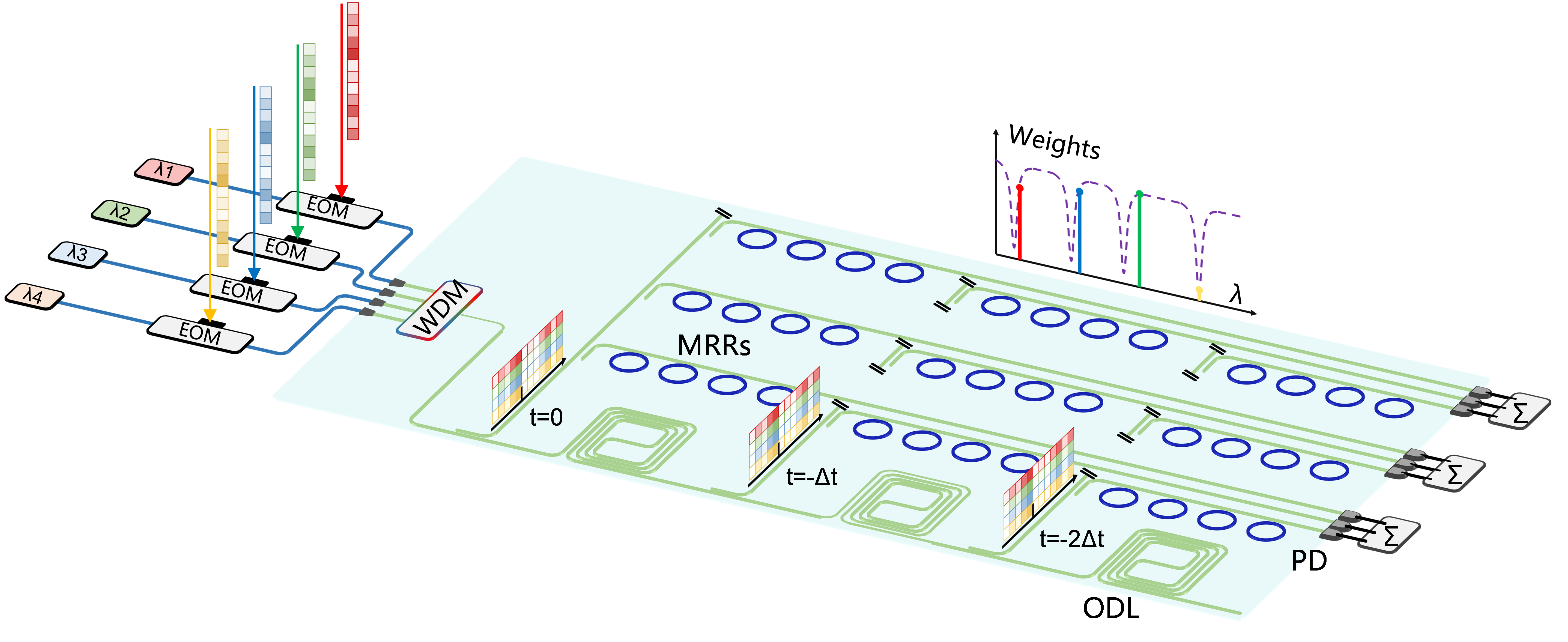
Figure 1 Architecture of the photonic tensor processing chip

Figure 2 The photonic tensor processing chip. (a) Packaged chip module. (b) Microscopic photo of the chip. (c) Wavelength response of the wavelength multiplexer. (d) Wavelength response of the microring array.
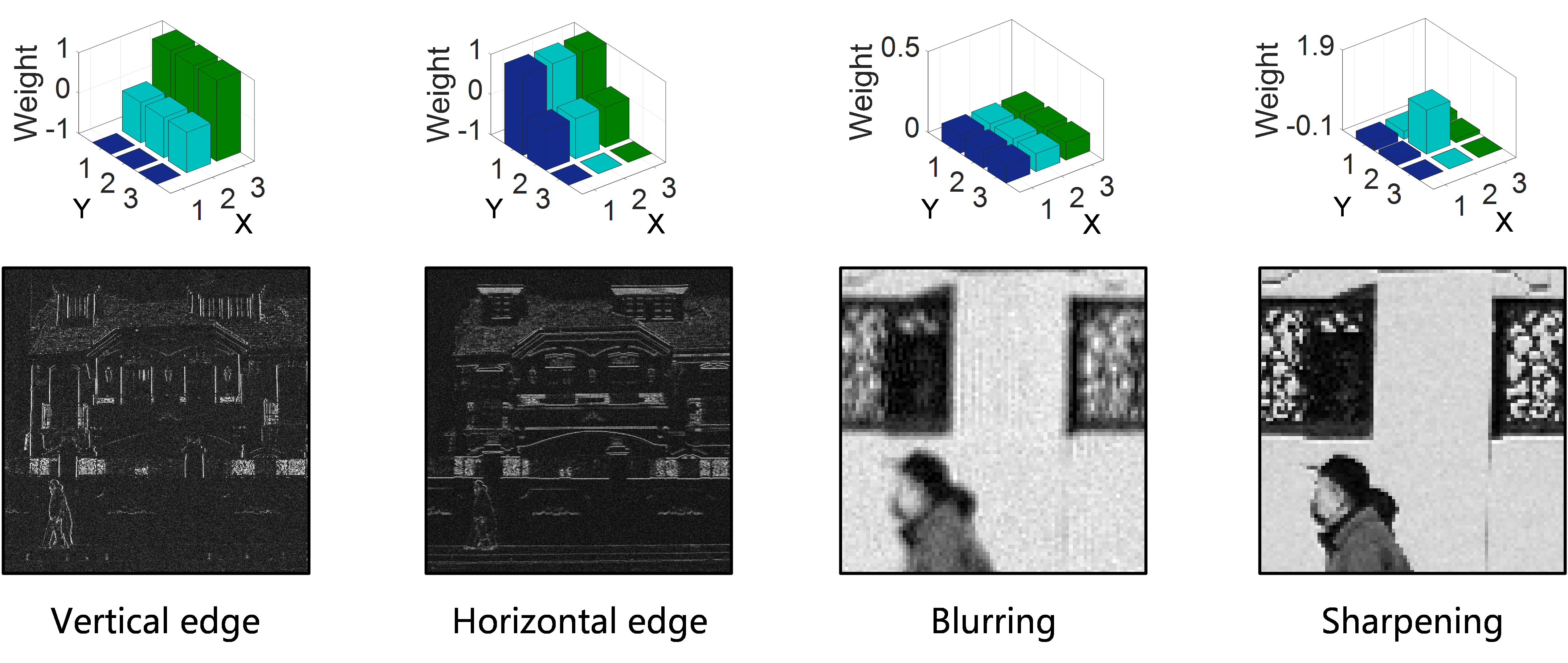
Figure 3 Result of multi-channel image convolution.
Related works
Prof. Weiwen Zou's group has conducted in-depth research in the direction of photonics-based computing and has developed the principle of optoelectronic processing and optoelectronic hybrid integration approaches to provide an important foundation for the successful development of this photonic tensor processing chip. Recently, they have conducted a series of researches on the core principle of photonic computing, innovative architecture, and advanced applications. Related papers have been published such as Opt. Express 2022, 30(23): 42057, Opt. Lett. 2022, 47(24): 6409. This research has also contributed to the successful development of the microcomb-based integrated photonic processing unit (led by Prof. Xingjun Wang's group at Peking University with the participation of Prof. Weiwen Zou's group), also published in Nature Communications recently,Nature Communications volume 14, Article number: 66 (2023).
Article information
Shaofu Xu, Jing Wang, Sicheng Yi, and Weiwen Zou, High-order tensor flow processing using integrated photonic circuits, Nature Communications 13, 7970 (2022), funded by National Key Research and Development Program (2019YFB2203700) and National Natural Science Foundation of China (T2225023, 62205203).
-
Link to the paper: https://www.nature.com/articles/s41467-022-35723-2.
-
Nature Communications is an international peer-reviewed multidisciplinary open access journal dedicated to publishing high-quality research in a variety of fields including biology, medicine, health, physics, chemistry, and earth sciences.